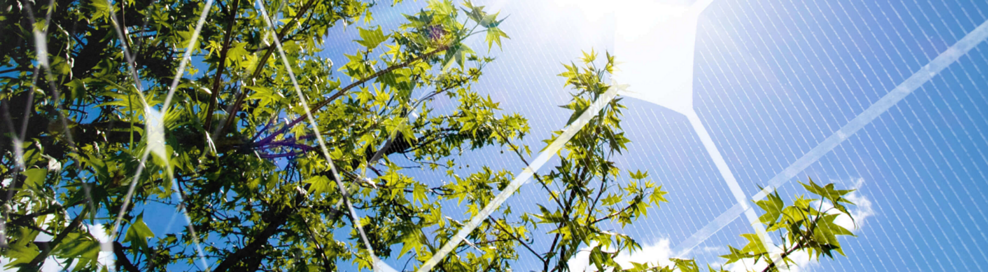
For more than 30 years, the diverse possibilities of optics for inspection and processing have inspired our innovations and technologies. Precision optical systems, consisting of lenses and lighting, combined with our application expertise and the right image processing system, make Vision & Control the ideal partner for the semiconductor and electronics industry.

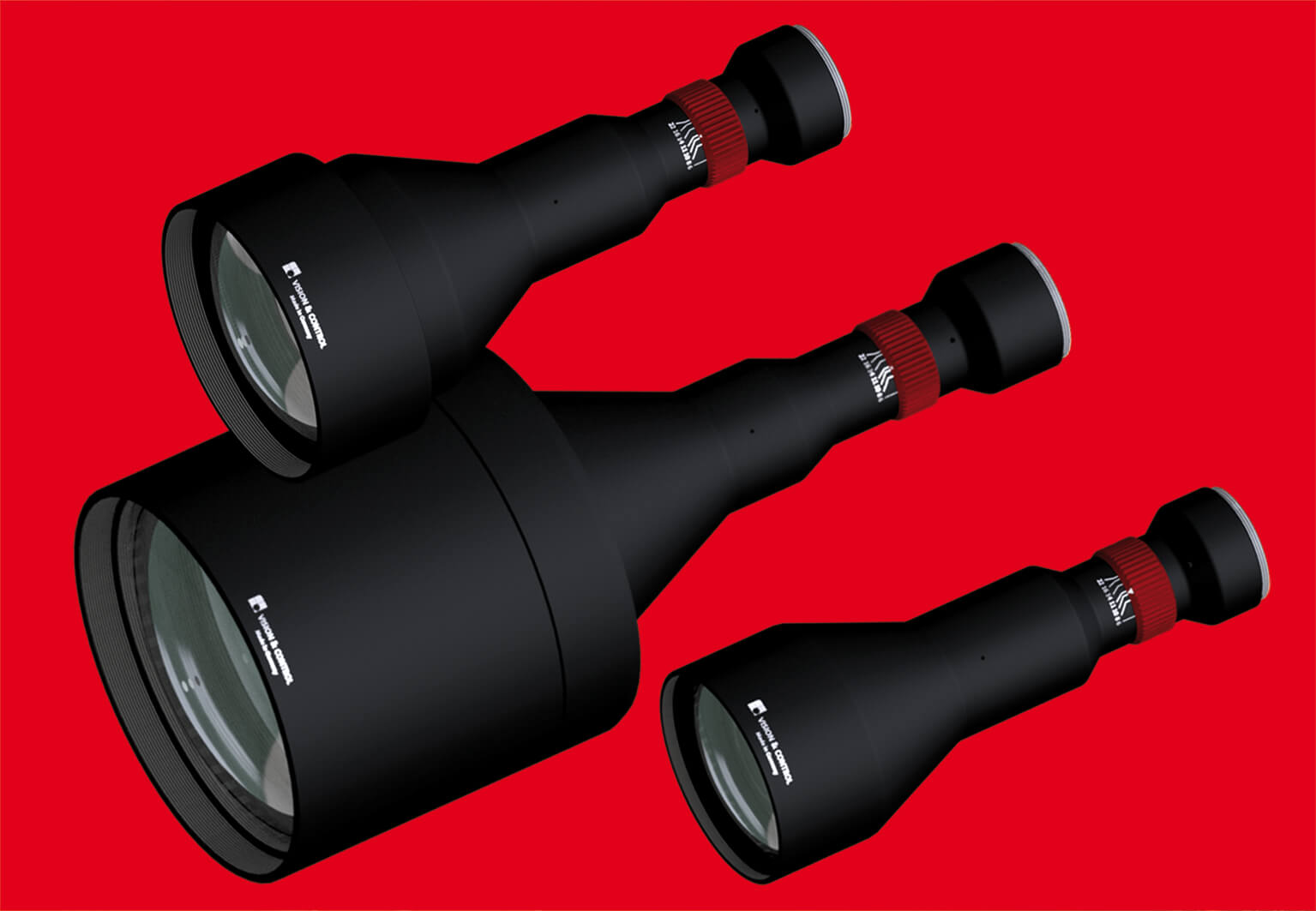
Suitable lenses for your application
A comprehensive catalogue of
- telecentric measurement lenses,
- telecentric wide field lenses,
- microscopic lenses
- and entocentric lenses, combined with custom specific lens development or modification to your requirements within shortest time to market and moderate batch numbers
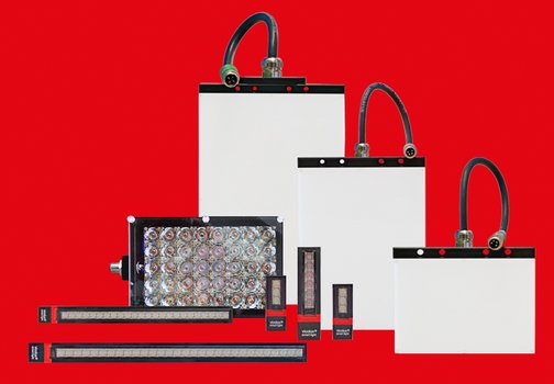
The suitable illumination or your application
Vision & Control offers a comprehensive selection of telecentric illuminations, ring light, bar lights, back lights, spots and dome lights.
If there is no suitable solution, the illuminations can be modified for the specific requirements. The integration of the illumination in an optical system is another component of our OEM services.

The vision system vicosys®
- a warranty for innovative solutions with unique properties of light for semiconductor and electronics testing. Some phenomenons become only visible with applied science in background.
Our application team appreciates to supports you with the realization of your inspection tasks.
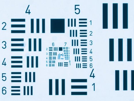
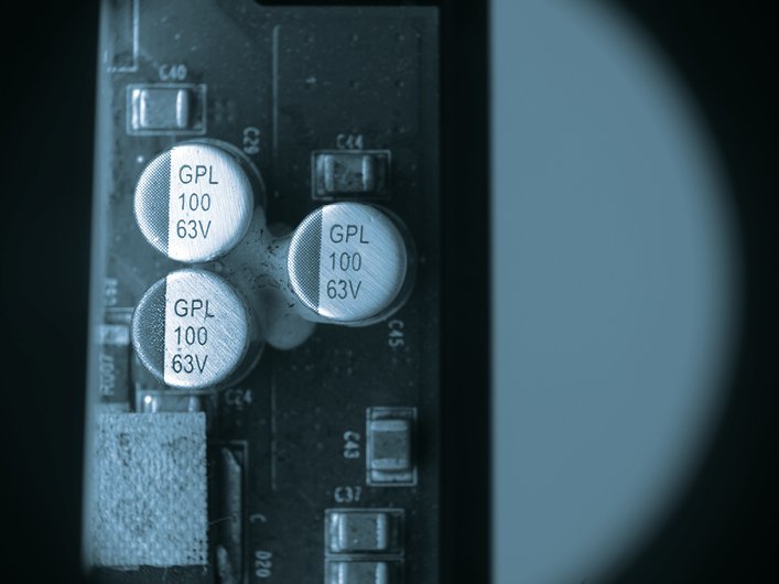
Highest precision in the measurement of structures, dimensions and positions of semiconductors, wafer components as well as printed circuits is achieved by combination of telecentric lenses and the suitable illumation.
Also, with optical critical surfaces and optical active materials the special solutions of Vision & Control lead to terrific solutions.
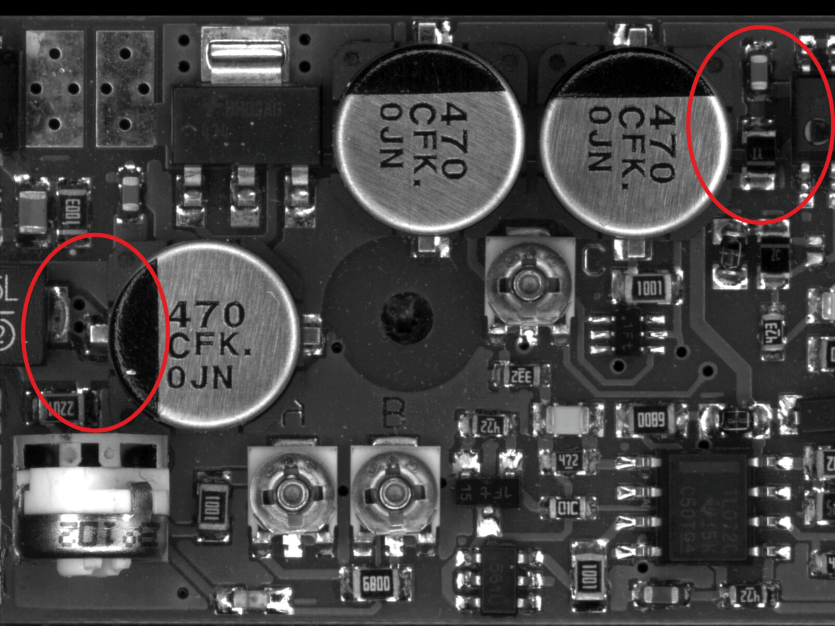
Using the advantages of telecentric optics and suitable illumination, different component heights on printed circuit boards (PCBs) with electronic components can be perfectly analyzed without having to accept edge overlaps or change the viewing angle.
Depending on the inspection focus, the display of shiny structures with rounded surfaces or miniature sinks can be easily integrated into the same inspection step by combining homogeneous incident light illumination and coaxial reflection of the illumination into the beam path of the lens.

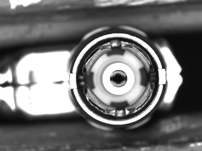
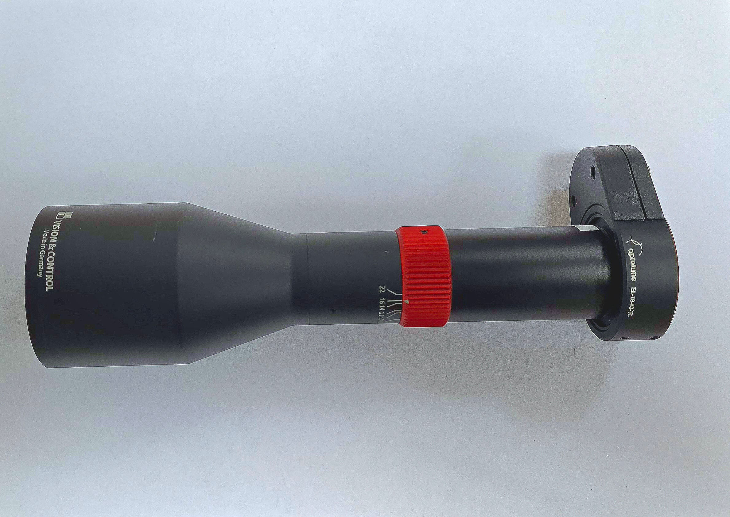
Depending on the size and depth of the contact area, a special depth of field or adjustment of the working distance or focus may be necessary to ensure the required imaging quality over the entire area. This challenge can be met by integrating a liquid lens module into the optical system.
By using the I2C interface of the camera to the liquid lens module, the calibration of the focus to the sharpest image setting or targeted adjustment of the working distance can be controlled by GenICam commands from the vicosys® image processing system. This solution provides Vision & Control from a single source.
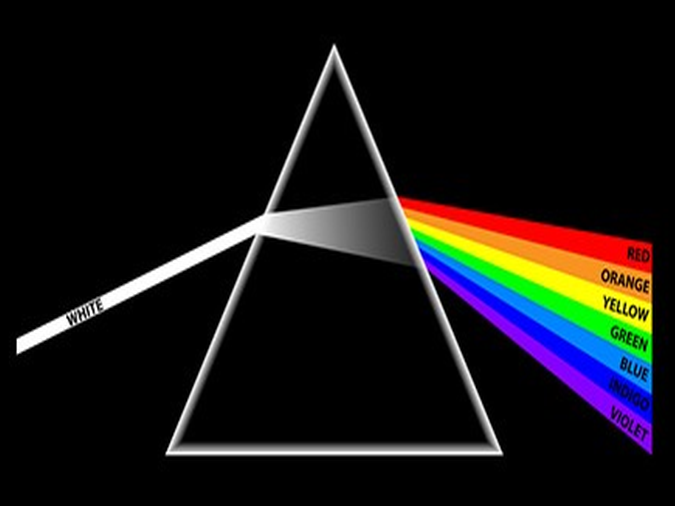
Use the wavelength-specific reflection of materials, especially in the short-wave infrared range (SWIR), to visualize hidden structures in semiconductor materials or transparent structures on the surface. This is made possible by imaging and processing in the SWIR wavelength range. Vision & Control develops, manufactures and supplies the appropriate optics, cameras and vicosys® image processing systems.
It is essential that the optical system can realize both the appropriate chromatic correction and the optimum transmission in the customer's focal wavelength range. Our application team will be happy to support you in the realization of your testing tasks.


Also using the infrared radiation of hot bodies, thermal inspection with corresponding thermal cameras (microbolometer cameras) offers the possibility of realizing both optical inspection tasks and the precise measurement of temperatures and temperature gradients. This technology is based on the detection of infrared radiation in the MWIR and LWIR wavelength range.
In combination with the thermography function of our vicosys® image processing systems, thermography inspections can be implemented and transmitted to the system control via an interface. Another outstanding field of application is the temperature monitoring of automated processes.
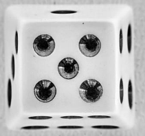
Optics with a pericentric perspective allow the inspection and measurement of surface structures and height differences. By precisely coordinating lighting, optics, the camera and the vicosys® image processing system, this profile data can be made measurable by certain calculations in the background.
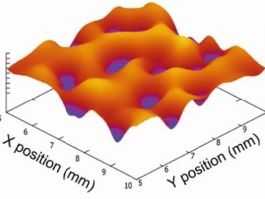
Another possibility to display height differences in the most precise scaling is the use of lenses with a very shallow depth of field and high numerical aperture (NA), e.g. to ensure the most precise height measurements in addition to other perspectives with only one lens in the “Depth from Focus” method.
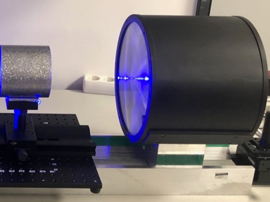
The use of large field lenses and corresponding large telecentric illuminators enables the telecentric inspection and alignment of panels or wafers as a whole.
Depending on the specific application, our large field lenses in Fresnel technology are used for different sensor sizes and image field sizes.


Additional Products
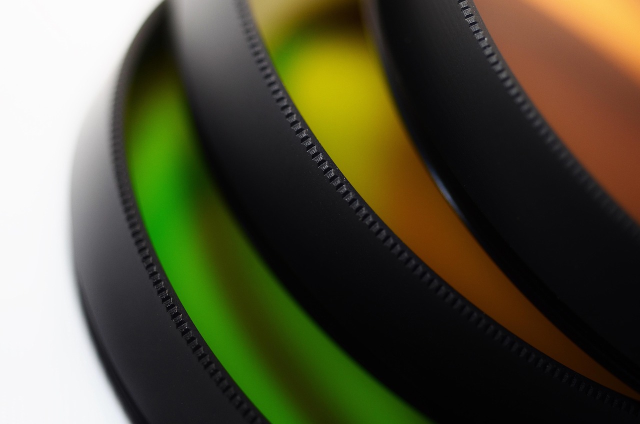
Microbolometer cameras, polarization filters and other filters (IR filters, ND filters, colour filters, UV blocking filters) can be found either directly assigned to the respective product or via our product search.
Further technical information on our vision systems or thermography.
![[Translate to English:] DIN Logo](/fileadmin/user_upload/Ueber_uns/Verbaende/DIN_Mitglied.jpg "[Translate to English:] DIN Mitglied")
![[Translate to English:] Logo Profinet](/fileadmin/user_upload/Ueber_uns/Verbaende/PROFINET_rgb..jpg "[Translate to English:] Mitglied PROFINET")
![[Translate to English:] Logo Optonet](/fileadmin/user_upload/Ueber_uns/Verbaende/OptoNet-Signet_sRGB_transp_800px.png "[Translate to English:] Mitglied OptoNet")