
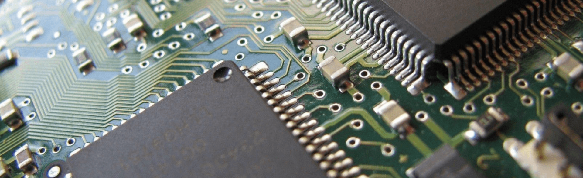
For more than 30 years, the diverse possibilities offered by optics for inspection and processing applications have inspired our products. Optical systems consisting of lenses and lighting, combined with our application expertise and the right image processing system, make Vision & Control your innovative partner for the electronics industry.

Making Hidden Structures Visible
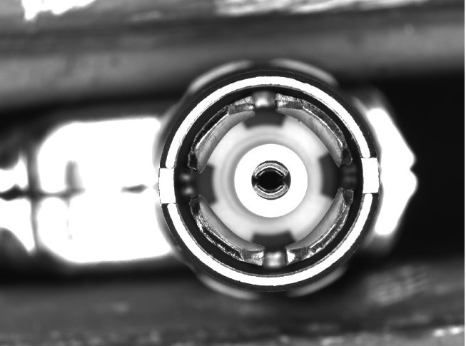
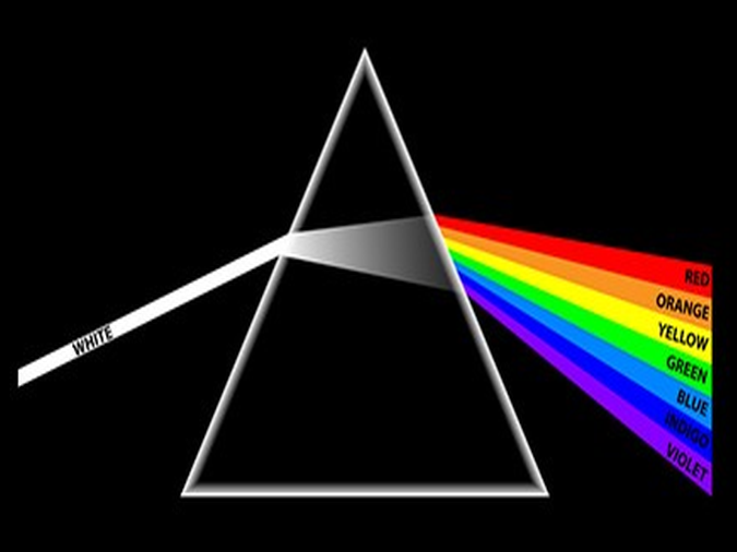
Take advantage of the wavelength-specific reflection of materials, particularly in the short-wave infrared (SWIR) range, to reveal hidden structures on printed circuit boards. This is made possible by imaging and image processing in the SWIR wavelength range. Vision & Control develops, manufactures, and supplies the appropriate optics, cameras, and vicosys® image processing systems for this purpose.
It is essential that the optical system be capable of providing both the appropriate chromatic correction and optimal transmission in the focal wavelength range.
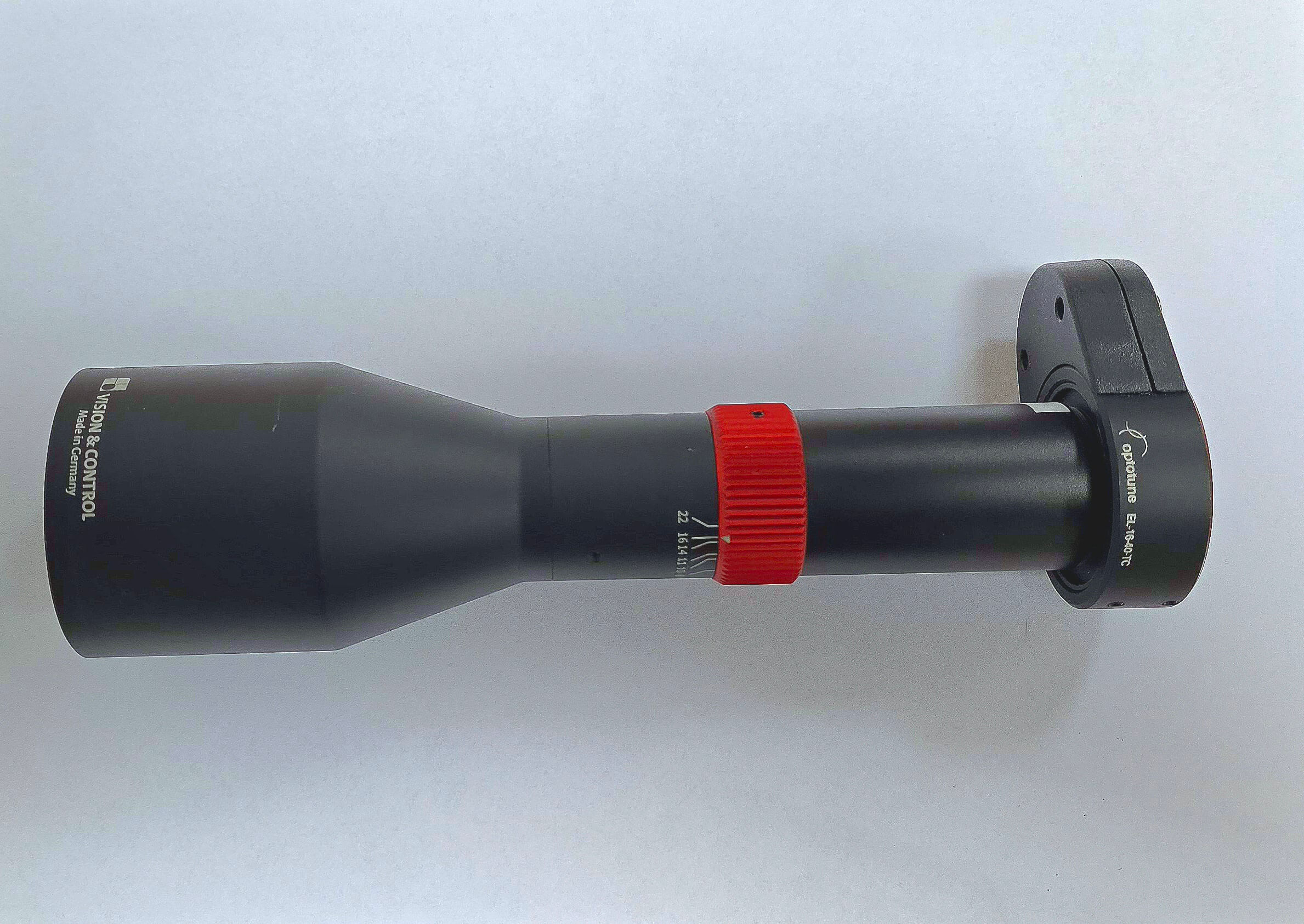
Quick adjustment of the working distance—e.g., during alignment processes
Depending on the size and depth of the contact area, a specific depth of field or adjustment of the working distance or focus may be necessary to ensure the required image quality across the entire area in every case. This challenge can be addressed by integrating a liquid lens module into the optical system.
By using the camera’s I2C interface to communicate with the liquid lens module, the vicosys® image processing system can control the focus adjustment to achieve the sharpest image or make precise adjustments to the working distance using GenICam commands. This solution provides vision and control from a single source.
Assembly Inspection and Orientation Check
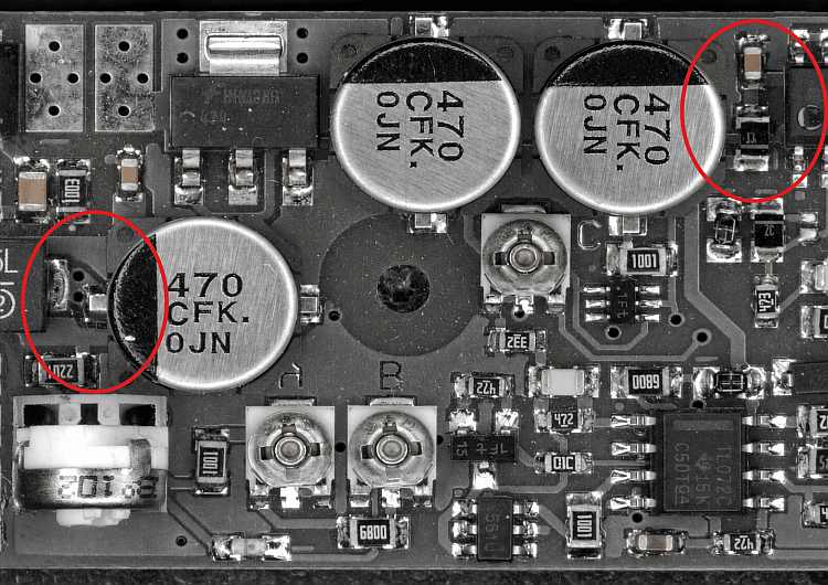
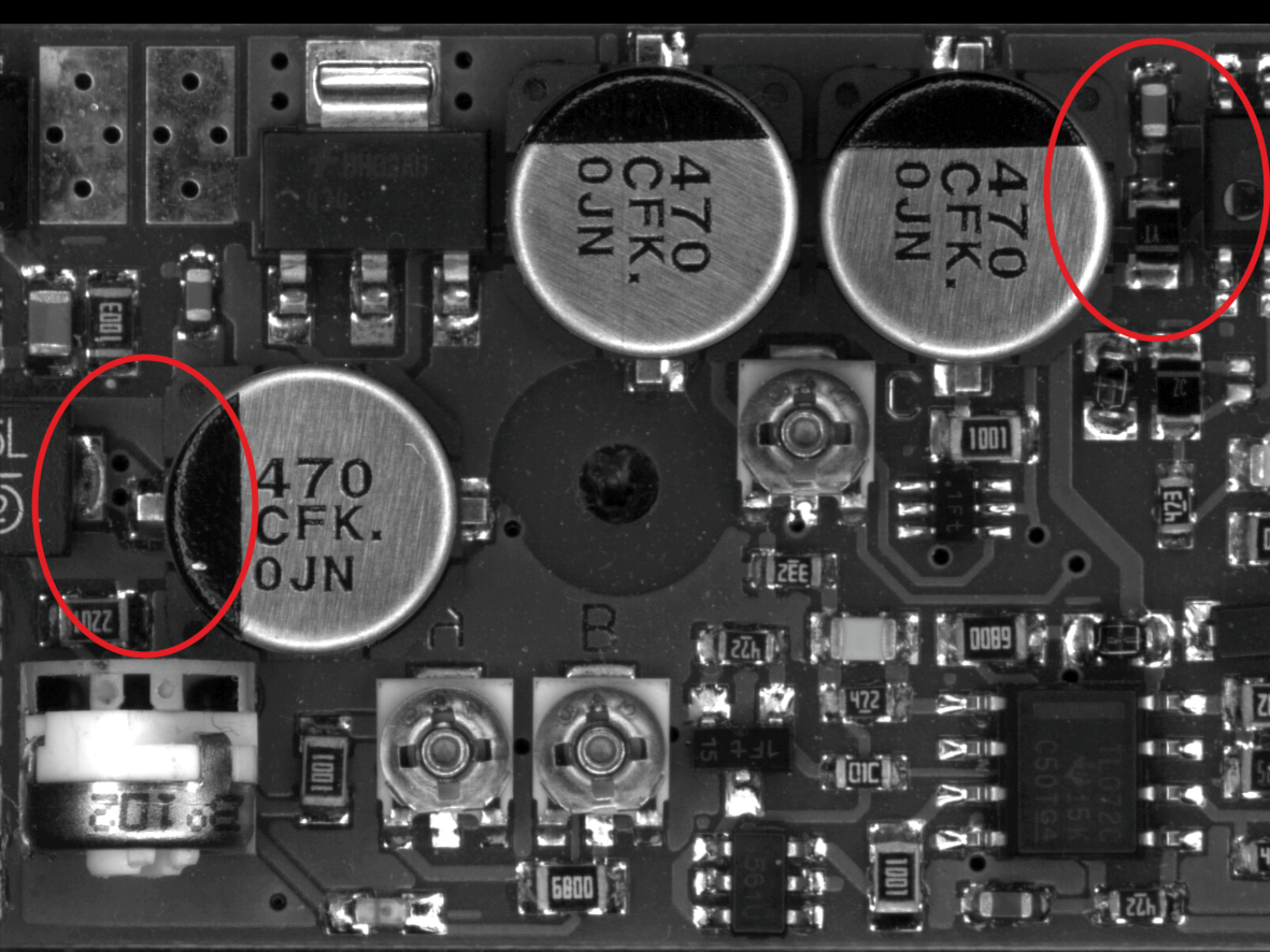
By specifically leveraging the advantages of telecentric optics and appropriate lighting, different component heights on printed circuit boards (PCBs) with electronic components can be perfectly analyzed without having to accept edge overlap or change the viewing angle.
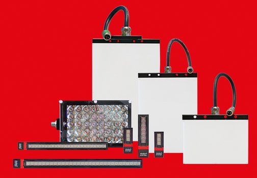
Depending on the focus of the inspection, the visualization of glossy structures with rounded surfaces or minisks can be easily integrated into the same inspection step by combining homogeneous incident light illumination with the coaxial reflection of the light into the lens’s optical path.
Localized, high-precision thermographic inspection of PCBs
Also using the infrared radiation of hot bodies, thermal inspection with corresponding thermal cameras (microbolometer cameras) offers the possibility of realizing both optical inspection tasks and the precise measurement of temperatures and temperature gradients. This technology is based on the detection of infrared radiation in the MWIR and LWIR wavelength range.
In combination with the thermography function of our vicosys® image processing systems, thermography inspections can be implemented and transmitted to the system control via an interface. Another outstanding field of application is the temperature monitoring of automated processes.

Highly accurate altitude measurements
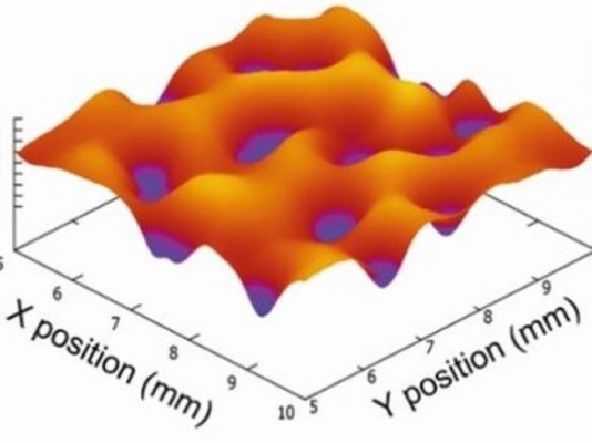
Another possibility to display height differences in the most precise scaling is the use of lenses with a very shallow depth of field and high numerical aperture (NA), e.g. to ensure the most precise height measurements in addition to other perspectives with only one lens in the “Depth from Focus” method.
Benefits as a whole
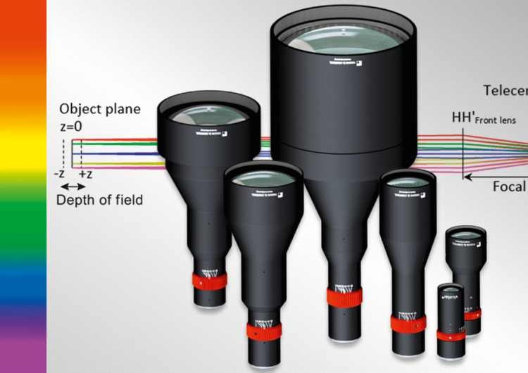
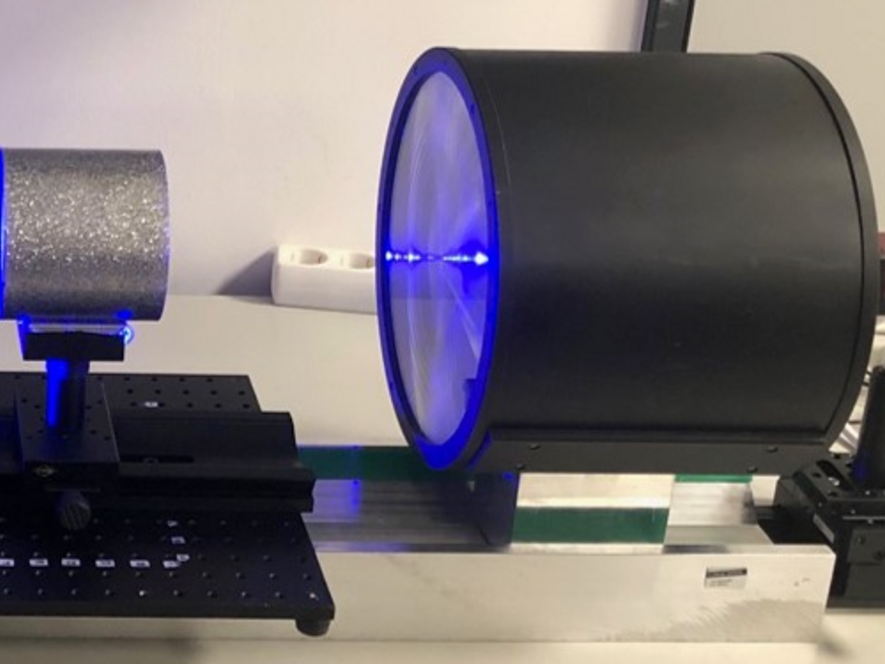
The use of large field lenses and corresponding large telecentric illuminators enables the telecentric inspection and alignment of panels or wafers as a whole.
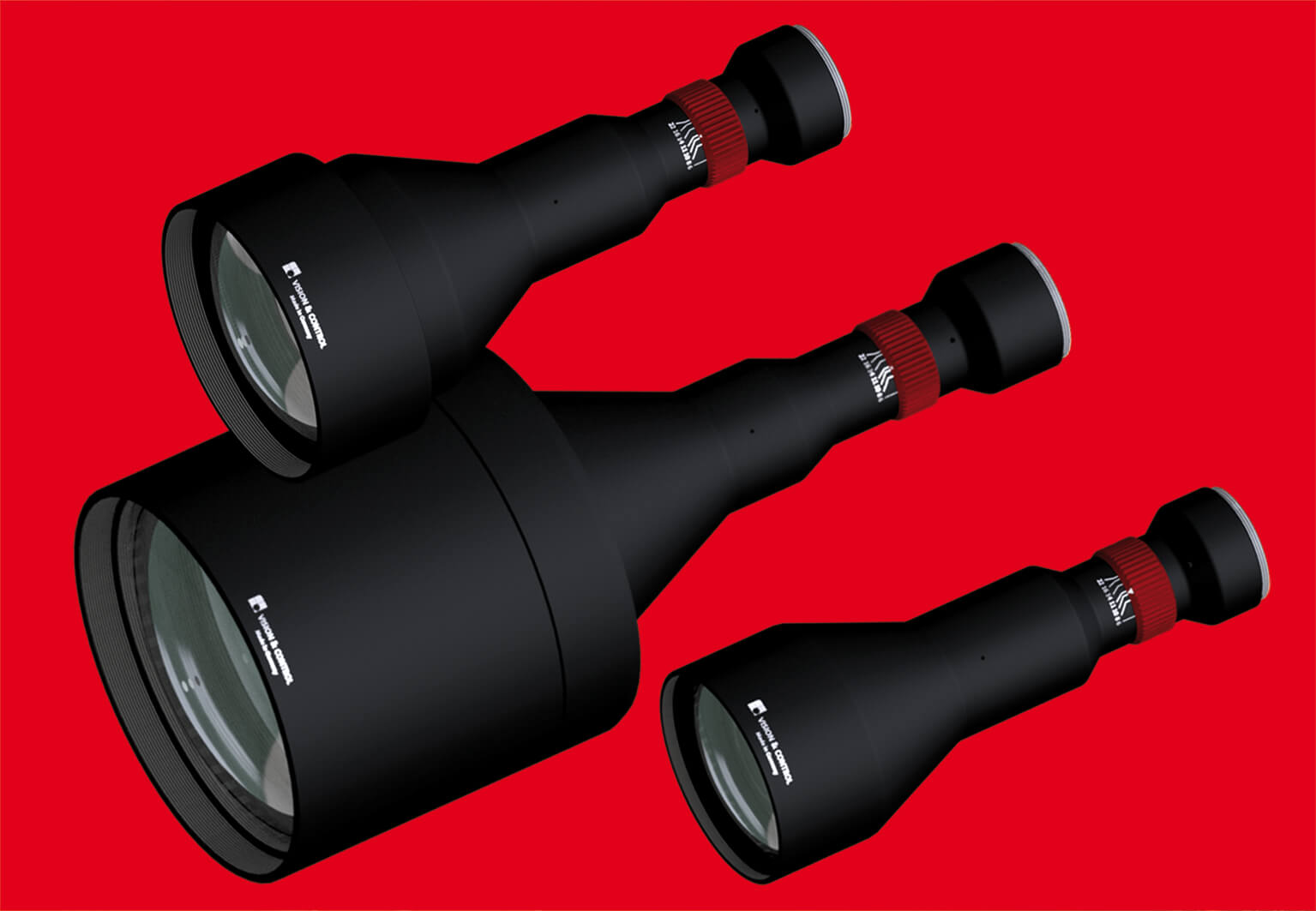
Depending on the specific application, our large field lenses in Fresnel technology are used for different sensor sizes and image field sizes.

The vicosys® image processing platform
- ensures that the unique properties of light are successfully implemented in industrial-grade applications for electronics and product electronics.
The vicosys® family enables innovative machine concepts based on a process-stable Linux operating system and industrial communication (EtherCat, PROFINET, I/O).
It also offers the option of integrating tried-and-tested libraries and algorithms, e.g. based on Python and Halcon.

![[Translate to English:] DIN Logo](/fileadmin/user_upload/Ueber_uns/Verbaende/DIN_Mitglied.jpg "[Translate to English:] DIN Mitglied")
![[Translate to English:] Logo Profinet](/fileadmin/user_upload/Ueber_uns/Verbaende/PROFINET_rgb..jpg "[Translate to English:] Mitglied PROFINET")
![[Translate to English:] Logo Optonet](/fileadmin/user_upload/Ueber_uns/Verbaende/OptoNet-Signet_sRGB_transp_800px.png "[Translate to English:] Mitglied OptoNet")